LNA 144/430 MHz на MMIC SPF5122Z
The new project of US4ICI and UR7IJM is given for your attention. It is a low noise amplifier for 144 or 430 MHz bands. This amplifier particularity is that it has built on base of one chip which amplification is enough for the proper functioning of system antenna-LNA-feeding cable-transceiver. This microchip of RFMD company production is SPF5122Z. Its description could be found here. Amplifier is energized by 5V and S-parameters for it were taken for 5V mode from here.
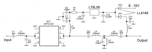
So let’s take a look to an amplifier in detail. 144 MHz LNA takes like an example. Schematic diagram of this device is provided on the Pic.1. As we can see, signal is going through matching circuit C1L1C2 and got to the chip input. It is amplified than and got to the band filter C4L4C5L5C6L6. A filter has losses less than 2 db. Filtered signal goes to the amplifier’s output and then to the feeder. Diodes VD1, VD2 are necessary for protection against wrong polarity and hitting of DC current to the feeder in case of amplifier energizing from external power source.

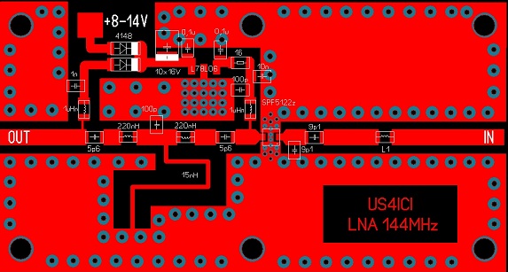
Circuit board size is 60×32 mm. It has made on double-sided FR-4 with thickness 1 mm, capacitivity 4.5, with apertures metallization and mask

LNA 144 MHz has following characteristics:
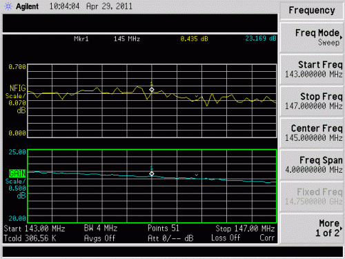
– gain factor better than 23 dB;
– noise ratio better than 0,45 dB;
– input VSWR not more than 1,6;
– OIP3 31,5 dBm;
LNA 430 MHz has following characteristics:
– gain factor better than 20 dB;
– noise ratio better than 0,55 dB;
– input VSWR not more than 1,8;
– OIP3 33 dBm.
Input power (transmitter power) on both bands should not exceeds 27 dBm. (Comparatively it transistors LNA input power should be less than 0 dBm). Any unstabilized power source from 8 to 15 V and 100 mA could be used for energizing of amplifier. In case design VHF energy can be supplied by feeder or separately through in-line filter.
Noise ratio and gain factor diagrams are represented on Pic. 3. They were taken by noise ratio measurer Agilent for 144 MHz band:

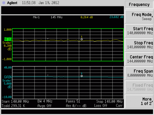
Following result was achieved after performing multiples experiments with purpose of input circuit optimization (Pic. 4.). It was done for 144MHz LNA with MMIC supply voltage 3V. Output circuit also was changed and has minimal loses on the main frequency.
