
Description
Sequencer has four outputs, which able to sink up to 50 V, 3 amps (P1-P4) and another output up to 30 V, 7 amps (P5) for LNA and RF Relays. Each output is protected from transient spike. The delay is adjustable (SW1 and SW2 jumpers on the board). Two jumpers let you set one of three delay values (SW1 – ON, SW2 – OFF; SW1 – OFF, SW2 – ON; SW1 – ON, SW2 – ON). The board has the LED’s allow a visual indication of timing for each port. The sequencer use a ground for PTT activation and simply can be activated from footswitch or PC interface. Each board is tested and ready to use. You just need to adjust the desired delay.
The sequence
- Initial state: PTT – OFF, P1-P4 – OFF, P5 – ON (12-27 V);
- TX – ON, RX – OFF (PTT to ground): EVENT 1 – P1 to ground, P5 – DC Power OFF -> EVENT 2 (active ground) -> EVENT 3 (active ground) -> EVENT 4 (active ground);
- RX – ON, TX – OFF (PTT not connected): EVENT 4 (active OFF) -> EVENT 3 (active OFF) -> EVENT 2 (active OFF) -> Event 1 (P1 – active OFF, P5 – DC Power ON).
Installation
The power line of LNA should be connected to port, which labeled as P5 (look at the picture). This output does provide +12 V on RX and 0 V on TX. Use this port for LNA and RF Relays. Please note, that in this case RF Relays will be supplied in RX mode. If you need for RF Relays voltage other than 12 V, remove the jumper (0 ohms resistor circled on the picture) and supply your desired voltage. Don’t exceed 27 V. Use additional IC Voltage regulator or DC-DC converter with 12 V output for LNA supply.
I recommend to perform a Pre-Check before installation.
The Pre-Check includes the following:
- apply voltage to the board at GND and +12 V points
- connect the PTT to ground and verify the TX sequence (listed above)
- verify the sequence on RX
- adjust a delay if it needs
- remove the DC power
This simple Pre-Check will show you how board is works. I have some cases where buyers damaged the board before installation and then reported the bad board. I strongly recommend to use a diode across all relays that you want to control from this sequencer.
Warning!
Don’t forget to remove 0 ohms resistor, if you want to supply P5 output from another voltage source.
List of changes.
In current Sequencer PCB edition SW1 and SW2 switch have been removed in order to improve the reliability.
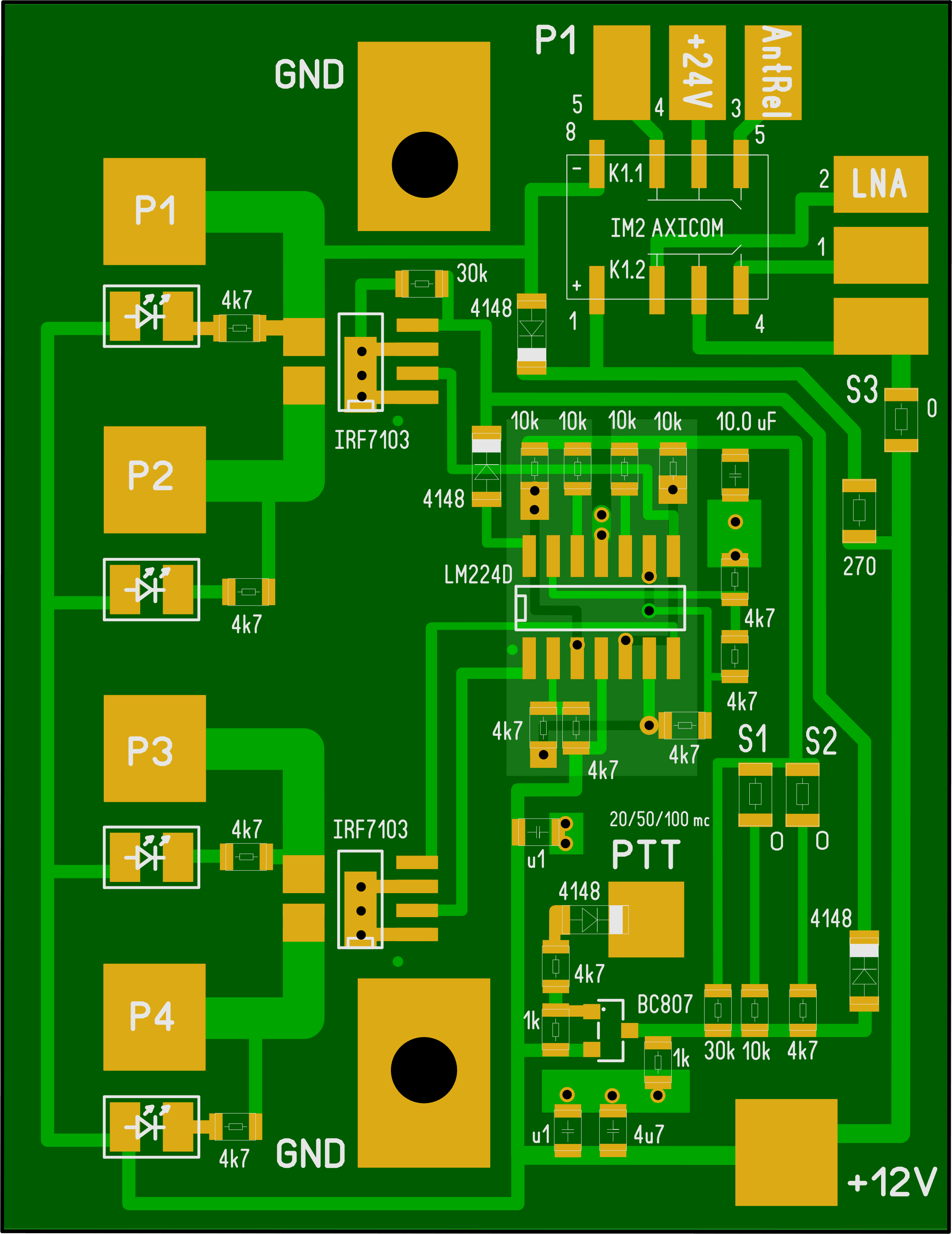
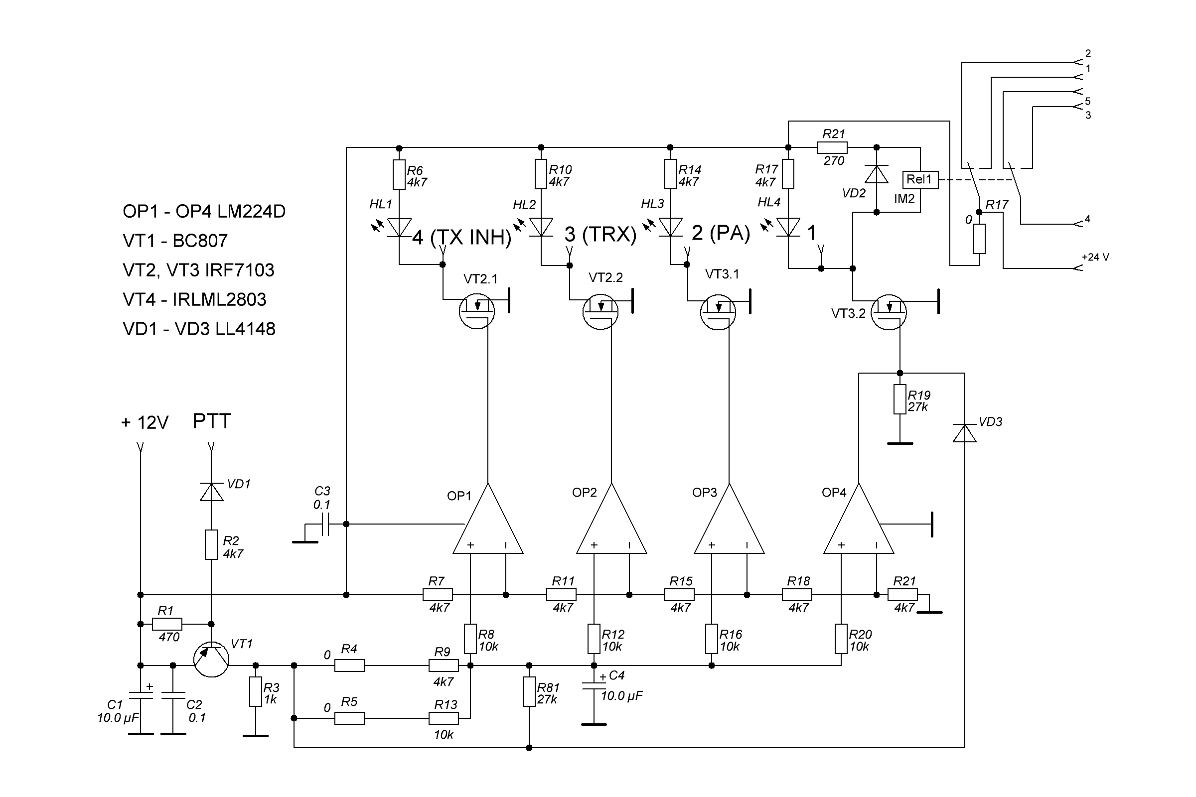
Schematic circuit is shown on Fig. 2

PCB layout on Fig. 3


(update from 2017-10-19)

(update from 2018-12-25)
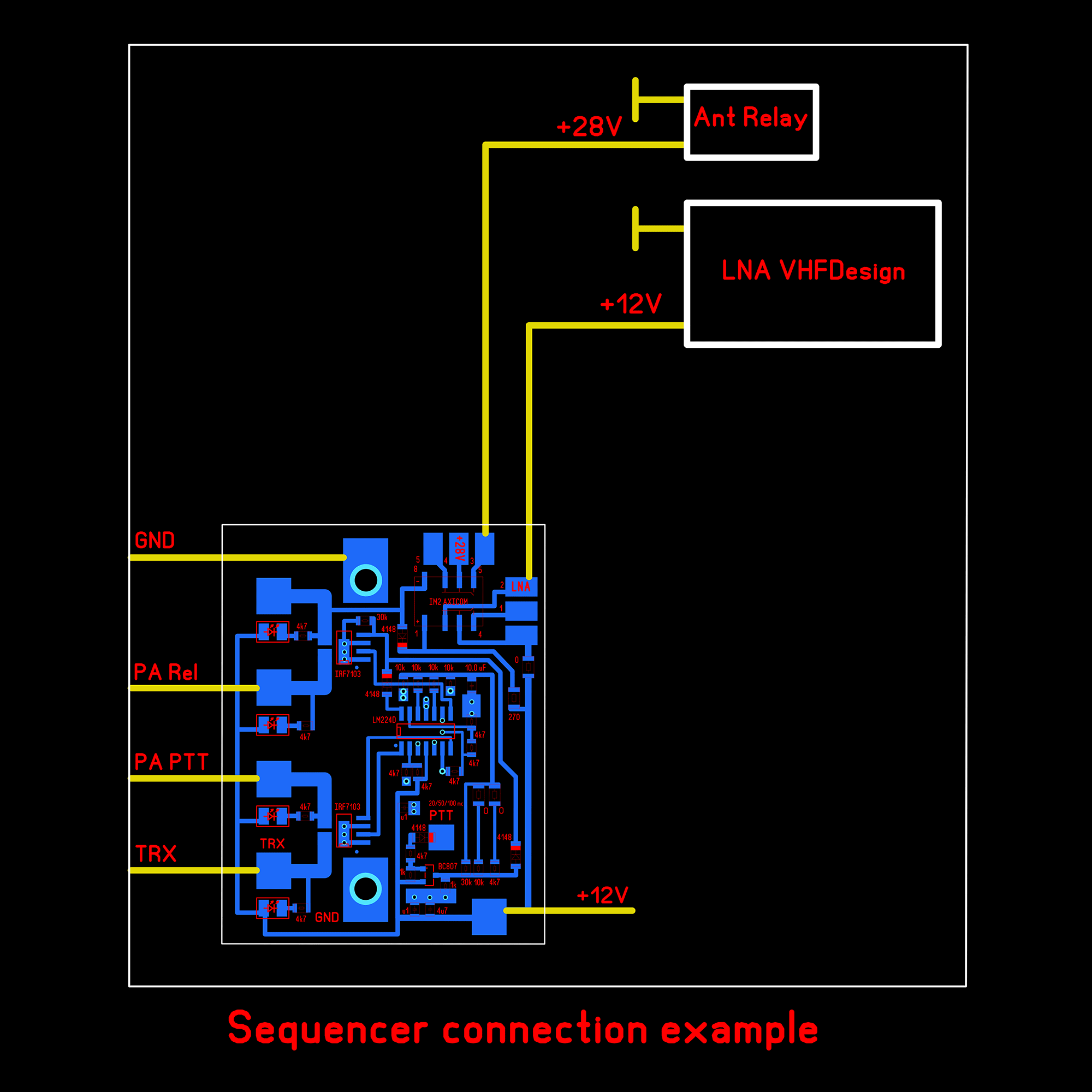
Sequencer’s connection example is shown on Fig. 4

Project update (up to date data)
Specifications
- Model: 5-ports-4-event-sequencer
- Board material: FR4 1.5mm
- Output: P1-P4 – 50V/3A(max), P5 – 30V/7A(max)
- DC voltage: 12V or 12V and 12-30V for P5 only
- Dimensions: 65 mm x 50 mm
- Assembled in Ukraine
Package includes
- 1 x 5-ports-4-event-sequencer
General inquiries:
![]() admin@vhfdesign.com
admin@vhfdesign.com
Technical support:
![]() us4ici@vhfdesign.com
us4ici@vhfdesign.com
Check the availability:
https://vhfdesign.com/kits/list
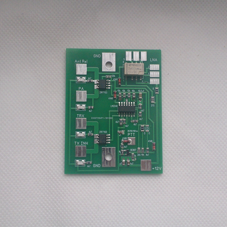
Appearance


