The history of synthesizer creation
In the process of searching of inexpensive solution for the LO SHF transverter, I drew attention to the ADF4350. The development of Analog Devices is well known and has been used for a long time in the developments of radio amateurs, for example this one.
PLL contains 2200 — 4400 MHz VCO. VCO frequency divider (multiple of 1/2/4/8/16) allows to synthesize frequencies from 137.5 MHz to 4400 MHz. A good phase noise (approximately -100 dBc/Hz, 10 kHz at a frequency of 1152 MHz). This development designed to be used as SHF LO (beacon, transverter) at a fixed frequency. Recommended frequencies range is between 550 and 4400 MHz. In case of using VCO divider more than /4 you need to take care of filtering the output signal.
PLL development
For the software development development board was purchased. The board contains a 25 MHz reference oscillator and requires an external controller to control the registers. AVR Attiny13 was used as an external controller. The program is written on C language for AVR and allows you to record up to 4 frequencies, which are selected by two jumpers (marked on PLL schematic as S1 and S2 jumpers).
PCB-LO-PLL-ADF4350 schematic diagram is shown on Fig. 1. Please note the location of S1 and S2 jumpers (0 Ohm resistors that configure 1 of 4 installed in Attiny firmware fixed frequencies) and location of R14 (0 ohm resistor, should be unsoldered in case you want to connect your own external reference).
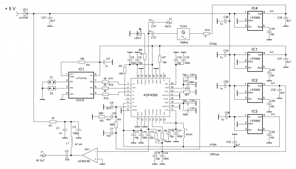
The schematics corresponds to the Analog Devices recommendations. In-circuit programming of the controller is provided. Four LP2992 regulators are used as voltage stabilizers. This voltage stabilizers make it possible to fully realize the PLL chip characteristics guaranteed by the manufacturer (phase noise, spurs). AG303-86 located at the output of the synthesizer. The “PLL lock state” indicates by the on-board LED. For an external reference oscillator an input is provided.
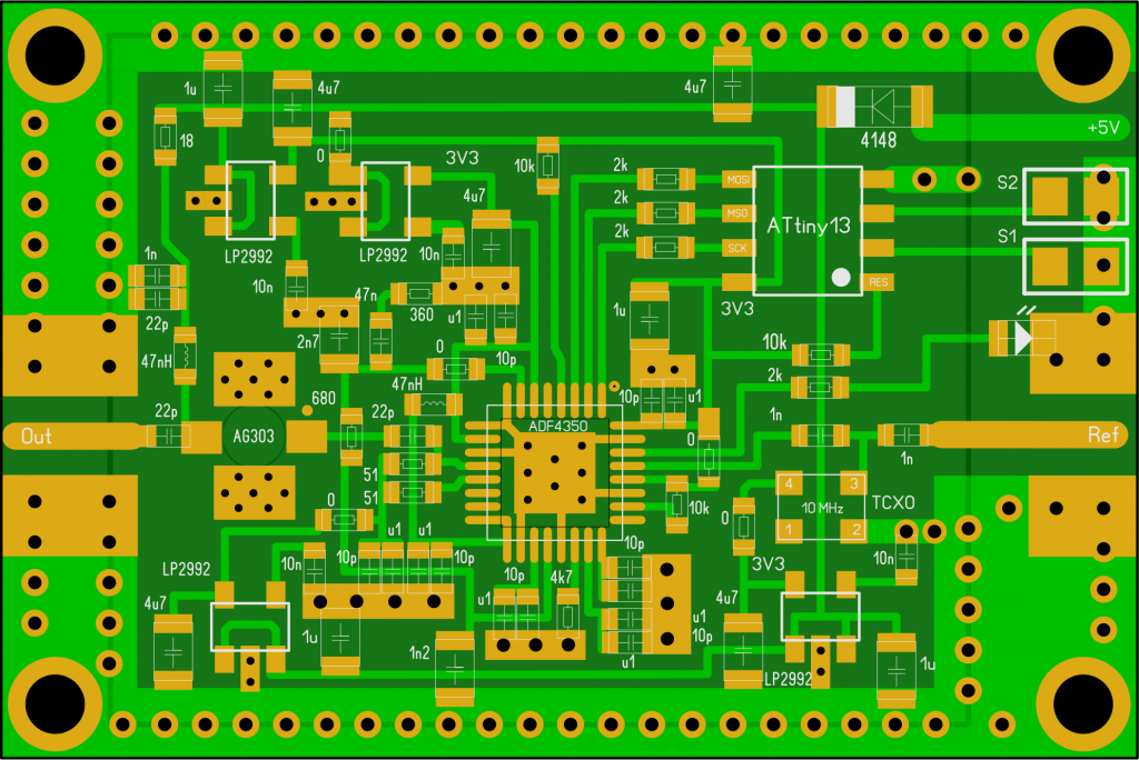
Printed circuit board (42 x 28 mm) made on FR4 1 mm with metallization of the holes and a mask. Protection cover goes with PLL PCB KIT. Board DC supply is 5 V (+/- 10%), current is less than 140 mA. For PCB mounting into the housing 4 holes (M2 screws) are provided. Housing should provide the heatsink features. With soldered protection cover you should be able to configure S1 and S2, supply the board with 5 V, connect the external reference oscillator, check the “phase lock” state. For in-circuit Attiny programming protection cover should be removed. It is convenient to use a soic8-sop8 adapter for in-circuit Attiny programming.
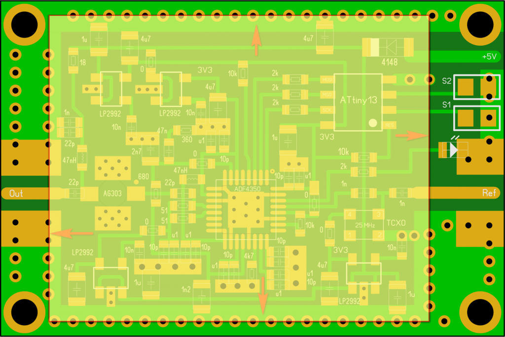
The coverage area of the protection cover is shown on Fig. 2.2
PLL frequency stability and phase noise depends of reference oscillator specs. Possiblie frequency range for Attiny programming is between 10 and 250 MHz, stability not worse than -130 dBc/Hz, 1 kHz. For internal on-board reference we used a TCXO type reference with the following specs: 0.5 ppm, -20 +70 C°, 10.000 MHz, SMD dimensions 3.5 х 2.7 х 0.9 mm. It should be enough for a home beacon, transverter 23cm tropo application. For SHF above 23cm, EME WJST – internal reference with better stability is recommended.
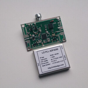
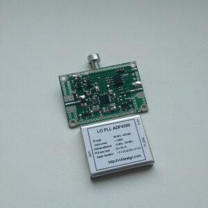
PCB-LO-PLL-ADF4350 comes in two editions: with on-board TCXO and without it. PLL appearance – Fig. 3
PLL programming
Evgeniy Ulianov – description of PLL work and programming
Attiny programming requirements:
1. Recommended reference oscillator frequency range is between 10.000 and 25.000 MHz, minimal step is 100 kHz.
2. Recommended output fixed frequencies range is between 550.000 and 4400.000 MHz, minimal step is 10 kHz.
It is possible to declare a reference frequency for each output frequency. So, please format your request like:
F1 = 10.000@1151.000 MHz (remove both S1 and S2 jumpers, default configuration)
F2 = 10.000@1152.000 MHz (install S1 jumper and remove S2 jumper)
F3 = 10.000@1296.000 MHz (remove S1 jumper and install S2 jumper)
F4 = 10.000@1297.000 MHz (install both S1 and S2 jumpers)
Important note: registers should be loaded to ADF4350 after the reference oscillator start. Default delay is 500 ms. In case your external reference starts slower, delay should be adjusted in order to ensure the correct work of the PLL board.
The program is written on C language in the Atmel Studio 7.0 IDE. The compiler is GCC version 5.4.0.
Frequencies can be specified explicitly through the preprocessor #define directives. The reference oscillator frequency is setted up the same way.
With using the references with frequencies of 10.000 MHz, 13.000 MHz and 25.000 MHz, any output frequency in the range 550 – 4400 MHz (steps of 100 kHz) is guaranteed.
To set the output frequency with a smaller step or another, including a fractional reference frequency, you need to use the ADF435x which will help you calculate the corresponding INT, FRAC and MOD values for a specific output frequency with a specified reference frequency. In this case, it is also possible to set the output frequencies of the LO PLL for different reference frequencies.
After starting the ADF435x software you need to select our synthesizer chip – ADF4350 (in the “Select Device and Connection” tab) and then open the “Main Controls” tab.
Enter the required output frequency in the “RF Frequency” field. Enter the reference frequency in the “Reference Frequency” field. If an exclamation point appears in the yellow triangle next to any field – parameter is out of acceptable range. For example, the value of MOD was more than 4095. To solve this issue it is enough to change the value of the “Channel spacing” field (in most cases). When using the source code where the calculation is made from the explicit assignment of frequencies by the compiler preprocessor using integer arithmetic, it is strictly not recommended to change the 10 kHz step value.
You should remember that the possibility of dividing or multiplying the reference is not realized in the software. Also, the division of VCO more than by /4 is not realized too. At the same time, it is possible to fully control the operation of the synthesizer chip even in the absence of programming skills. In order to do this, it is enough to change (based on datasheet) the corresponding parameter values in the #define blocks describing the contents of the control registers of the synthesizer.
For example, to change the value of “R Counter” from 1 to 6, you must replace the line
#define ADF4351_R_COUNTER 1#define ADF4351_R_COUNTER 6You should remember that these changes will affect to all output frequencies!
The values of INT, MOD and FRAC calculated by the ADF435x sortware are entered into the definitions for the corresponding output frequency.
For example (F1 = 1152.030 MHz with 25 MHz reference frequency and the values INT = 92, FRAC = 203 and MOD = 1250):
#define ADF4351_INT_F1 92
#define ADF4351_FRAC_F1 203
#define ADF4351_MODULUS_F1 1250
It is necessary to specify the value of the frequency itself, since the corresponding VCO divider is set from this value:
#define FREQ1 1152030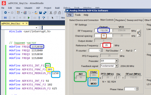
The source codes for the variant with automatic calculation (adf4350_tiny13a.c) and the variant with the direct input of INT, MOD and FRAC values (adf4350_tiny13a_nocalc.c) are here. The .hex firmware file for the 10 MHz reference frequency and output frequencies: 1151 MHz, 1152 MHz, 1296 MHz, 1297 MHz in the archive too.
It is necessary to program the fuses with the following values: low: 79, high: FF when flashing the microcontroller.
You can use any AVR compatible programmer for Attiny flashing, for example USBASP.
Information about using the programmer, installing and configuring the software, you can find in the internet.
To compile the firmware from the source code, it’s enough to create (in Atmel Studio 7.0 IDE) a new project “GCC C Executable Project”, select microcontroller type (attiny13a) and replace the contents of the automatically generated “main.c” file with the contents of the file from the archive that listed above. Then switch the configuration from “Debug” to “Release” and press the F7 (compile) button. If everything is done correctly, you can find ready for flashing .hex file in “Release” folder of the project.
In this software, the output frequency is set after the power is applied to the LO PLL board and after the jumper state that determines the output frequency is changed. The delay before loading data into the registers of the ADF4350 chip after the power supply is 500 ms.
It is possible to adjust the program for other tasks, for example scanning at two or four frequencies for a multi-band beacon.
| PCB LO PLL ADF4350 technical specifications | |
|---|---|
| RF range: | 550 — 4400 MHz |
| TCXO stability: | Typ. +/– 0.5 ppm -20 +70 C° @ 10 MHz |
| Pre-installed configuration: | F1 = 1151 MHz (used by default) F2 = 1152 MHz (configure S1 = ON, S2 = OFF) F3 = 1296 MHz (configure S1 = OFF, S2 = ON) F4 = 1297 MHz (configure S1 = ON, S2 = ON) |
| PLL SSB PN @ 10 kHz Offset: | -100 dBc/Hz at 1152 MHz |
| Output power: | > 10 dBm |
| DC voltage: | 5 V +/–10% |
| DC current: | < 140 mA |
| PCB dimensions: | 42 mm x 28 mm |
Frequencies can be programmed according to your requirements. Any combination of reference oscillator frequencies and output PLL frequencies is possible in the compatible frequency range, reference frequency range is between 10 and 25 MHz (minimum step is 100 kHz), the output frequencies range is between 550 and 4400 MHz (minimum step is 10 kHz). Some frequencies can be set to work with the on-board TCXO reference and others – to work with your own external reference. Please specify the reference frequency for each output frequency in this case.
Examples:
10.000@1296.000_1152.000_1268.000_2320.000 MHz
10.100@1296.010_1152.010_1268.010_2320.010 MHz
F1 = 10.000@1151.000
F2 = 25.000@1151.000
F3 = 10.000@1296.000
F4 = 25.000@1296.000