Transverter’s block scheme is shown on Fig. 1

How it works
Possible IF frequencies: 430/432/435 MHz (435 MHz by default). In RX Mode signal goes to high frequency amplifier that built on three active elements: 1 x HMC717 and 2 x Gali-39+.
High frequency amplifier’s parameters the following
- Gain: 48 dB
- Noise figure: < 1.5 dB
- OIP3: 20 dBm
Then signal goes to the Wilkinson’s bridge, which provides RX and TX paths decoupling and then goes through a 6th order microstrip filter to the passive double mixer HMC219, where he mixed with a synthesizer’s signal (5325 MHz). Dedicated IF signal (435 MHz) goes through the 3dB attenuator and relay to the transverter’s output. Relay is switched ON.
In TX Mode signal goes to the transverter’s input. Relay is switched OFF. IF signal goes to the powerful attenuator (25 dB, 5 Watt), which made on six SMD resistors (300 Ohms, 1 Watt). After this IF signal through the protection circuit (3 dB attenuator, LL4148 diodes) goes to HMC219 mixer, where he is mixed with frequency synthesizer. Microstrip filter allocates 6 cm band signal, which goes through the Wilkinson’s bridge to two-cascade RF amplifier, consisting of Gali-39+ and GVA-84+.
The sequencer is assembled on LM224D operational amplifier. He allows to provide switching sequence for RX/TX path, PA and ant. relay. For power switching of receiving and transmitting paths IRF7316 twin key is used. He is able to pass a current up to 3 A without appreciable case heating.
RF VOX delay in the transition to the TX mode based on NE555 timer. Thus, when telegraph key is accidentally pressed and IF goes to transverter input he automatically switches to transmit mode (RX VOX triggered) and will stay in this state for about 0.5 seconds.
RF Path and sequencer’s schematic circuit is shown in Fig. 2

In case of PTT input absence (in your PA) you need to assemble external PA’s power switching circuit. For this purpose it is desirable to use p-type MOSFET, IRF9540N for example, with 20 A maximum current.
Scheme’s inclusion is shown in Fig. 3

Under current commutation more than 2 A transistor must be installed on a small radiator. For example, PA consumes a current up to 5 A – aluminium plate (dimensions 80×50 mm) can be used as a radiator.
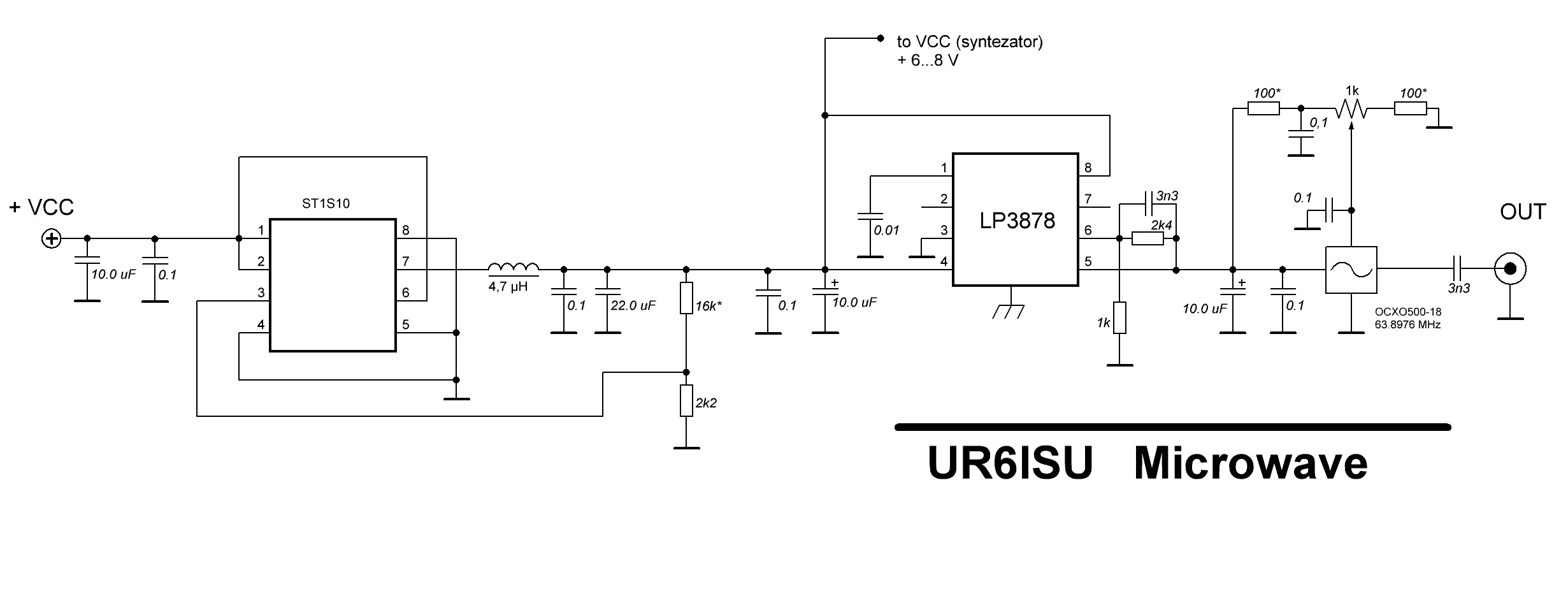
For synthesizer and local oscillator supply LP3878 stabilizers are applied. Schematic circuit is shown on Fig. 4
Transverter’s synthesizer is assembled on HMC840, US4ICI design. Schematic circuit is shown on Fig. 5

Synthesizer differs a low phase noise, that allows you to use transverter in a significant interference conditions. Synthesizer’s signal is enhanced by two cascades: Gali-39+ and GVA-84+. Control is organized by using ATtiny45 microcontroller. The program allows to set one of three frequencies by sealing a jumper from 2nd and 3rd processor’s legs.
Assembly options
- NO Jumper, 5325 MHz (IF = 435 MHz), default option;
- Jumper between 2nd processor’s leg and GND, 5330 MHz (IF = 430 MHz);
- Jumper between 3rd processor’s leg and GND, 5328 MHz (IF = 432 MHz).
We have come to the conclusion that the default IF frequency (435 MHz) is optimal, change isn’t recommended.
Choosing synthesizer frequency for different IF states
| Processor’s leg that should be connected with the GND | Synthesizer’s frequency (MHz) | IF frequency (MHz) |
| – | 5325 | 435 |
| 2 | 5330 | 430 |
| 3 | 5328 | 432 |
| 2+3 (both legs) | 5616 | 144 (not tested, not recommended) |
The LED on the synthesizer’s board under VCO frequency capture should light up.
Assembly materials
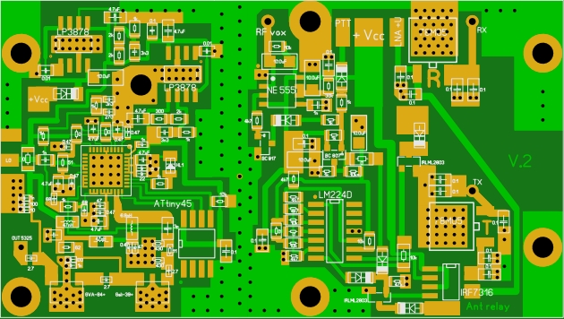
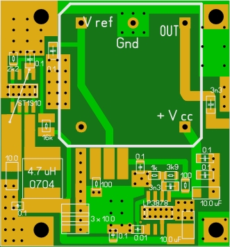
Main transverter’s board (RF part) – Rogers RO4003C 0.508 mm. Schematic circuits of synthesizer, sequencer and local oscillator – FR4 1 mm (Fig. 6.1, Fig. 6.2, Fig. 6.3).

Connection example is shown on Fig. 7

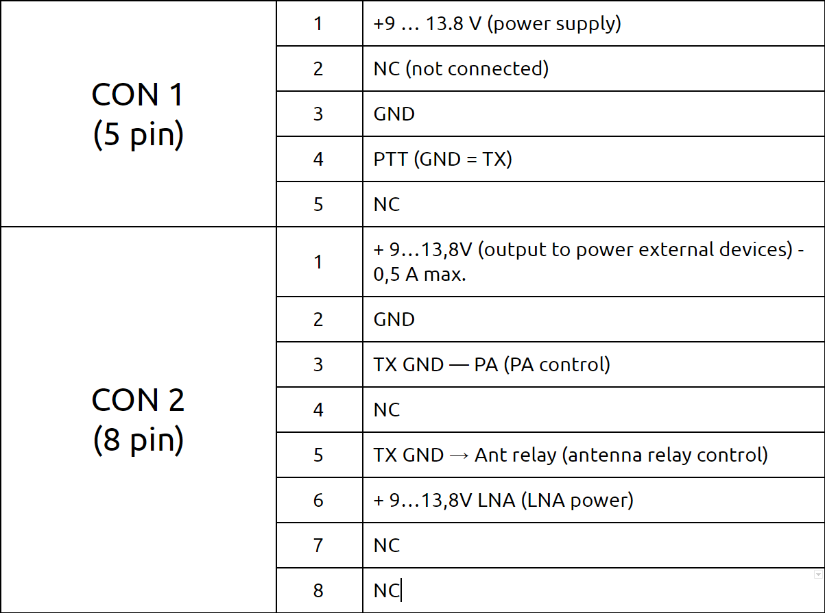
Annex 1. Supply and management pins assignment
Specifications
- Model: TRCV-6cm-70cm
- RF: 5760 MHz LO: 5325 MHz (by default)
- IF: 435 MHz (by default)
- Reference oscillator frequency stability (0 … 70 °C): typ. 0.2 ppm max
- PLL SSB PN @ 10 kHz Offset: -109 dBc/Hz
- Output power: > 13 dBm
- IF input power: 2 Watt (max 5 Watt SSB, CW)
- Noise figure: < 1.5 dB
- RF path gain: 48 dB
- DC power: + 9 – 13,8 V
- DC current: 0.5 A (TX) / 0.45 A (RX)
- Connectors type: SMA-female, 50 Ohms
- Dimensions: 165 x 65 x 28 mm (with connectors)
- Weight: 0.3 kg
- Assembled in Ukraine
Package includes
- 1 x TRCV-6cm-70cm
Appearance


